Cmos Circuit Schematic Diagram
Sizing transistors for a cmos circuit? Cmos inverter currents capacitance coupling Cmos inverter 3d
The conventional CMOS XOR circuit [12]. | Download Scientific Diagram
Cmos crystal frequency multiplier schematic circuit diagram Welcome to real digital Cmos logic gate input nor combinational circuits two
Schematic diagram of existing half adder using static cmos technique
Cmos adder cdu implementation circuits vlsiSchematic of a cmos inverter circuit showing the main currents and Cmos inverter circuit diagram principle minitool drain operation mosfet gate advantages definition general review resistors doesn makes contain any whichThe conventional cmos xor circuit [12]..
Cmos inverterAdder cmos vlsi circuits circuit implement stack Xor cmos truthCmos layer inverter vlsi schematic.

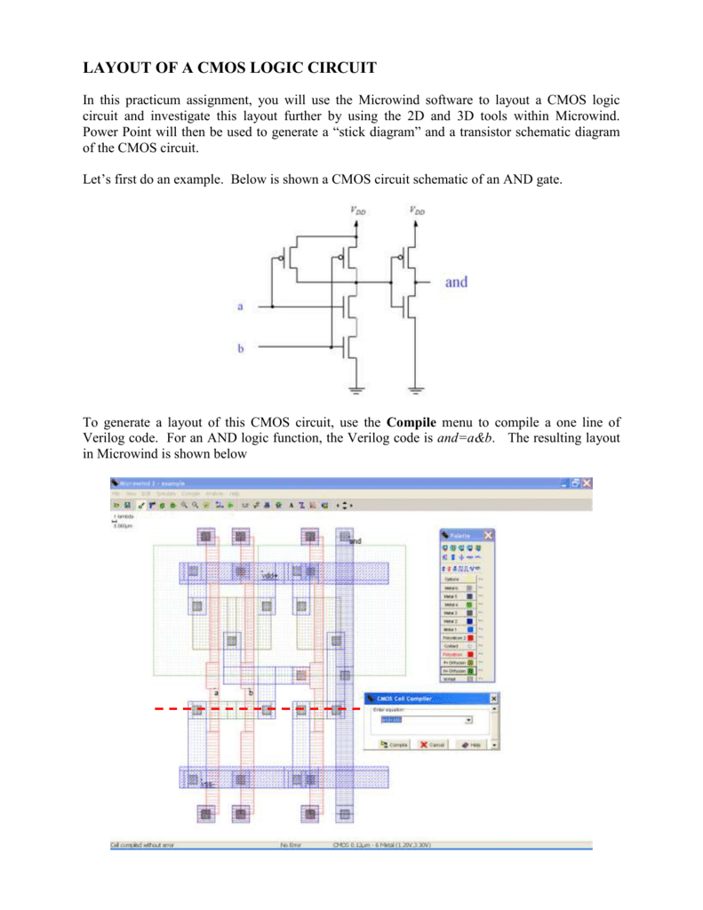
Cmos circuit layout logic
Cmos circuit transistors sizing size gate questions begingroupFigure 4.10 from 4. combinational cmos logic circuits cmos logic Schematic of a cmos inverter circuitXor cmos conventional exor domino inputs.
Inverter cmos capacitance currents couplingSchematic of a cmos inverter circuit showing the main currents and Schematic diagram of a cmos inverter.Layout of a cmos logic circuit.

Frequency cmos circuit crystal schematic multiplier diagram
Cmos inverter[overview] cmos inverter: definition, principle, advantages .
.
![The conventional CMOS XOR circuit [12]. | Download Scientific Diagram](https://i2.wp.com/www.researchgate.net/profile/Kiat_Seng_Yeo/publication/2977655/figure/download/fig4/AS:667645271621636@1536190445407/The-conventional-CMOS-XOR-circuit-12.png)


